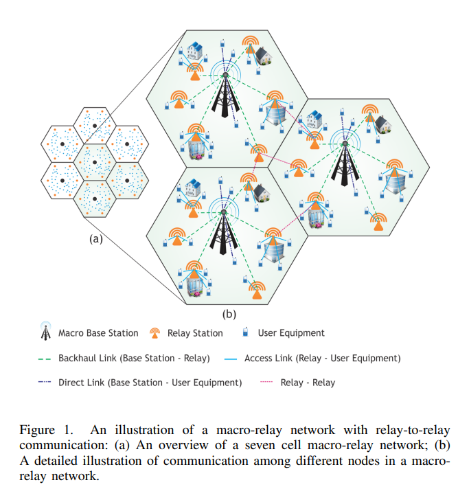
Towards energy efficient relay placement and load balancing in future wireless networks
This paper presents an energy efficient relay deployment algorithm that determines the optimal location and number of relays for future wireless networks, including Long Term Evolution (LTE)-Advanced heterogeneous networks. We formulate an energy minimization problem for macro-relay heterogeneous networks as a Mixed Integer Linear Programming (MILP) problem. The proposed algorithm not only optimally connects users to either relays or eNodeBs (eNBs), but also allows eNBs to switch into inactive mode. This is possible by enabling relay-to-relay communication which forms the basis for relays to
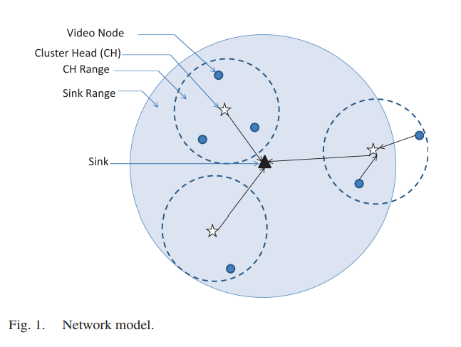
Optimal resource allocation for green and clustered video sensor networks
Wireless video sensor networks (WVSNs) are opening the door for many applications, such as industrial surveillance, environmental tracking, border security, and infrastructure health monitoring. In WVSN, energy conservation is very essential because: 1) sensors are usually battery-operated and 2) each sensor node needs to compress the video prior to transmission, which consumes more power than conventional wireless sensor networks. In this paper, we study the problem of minimizing the total power consumption in a cluster-based WVSN, leveraging cross-layer design to optimize the encoding power
Fractional-order bio-impedance modeling for interdisciplinary applications: A review
Bio-impedance circuit modeling is a popular and effective non-invasive technique used in medicine and biology to fit the measured spectral impedance data of living or non-living tissues. The variations in impedance magnitude and/or phase at different frequencies reflect implicit biophysical and biochemical changes. Bio-impedance is also used for sensing environmental changes and its use in the agriculture industry is rapidly increasing. In this paper, we review and compare among the fractional-order circuit models that best fit bio-impedance data and the different methods for identifying the
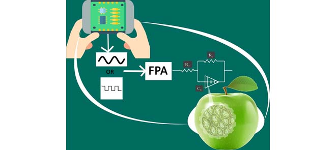
Extracting Optimized Bio-Impedance Model Parameters Using Different Topologies of Oscillators
This paper demonstrates the possibility of extracting the single-dispersion and double-dispersion Cole-bio-impedance model parameters using oscillators (sinusoidal or relaxation). The method is based on replacing selected components in the oscillator structure with the biological sample under test and then using the Flower Pollination optimization Algorithm (FPA) to solve a set of nonlinear equations in order to extract the unknown model parameters. Minimum component sinusoidal oscillators and relaxation oscillators are used in this work and experimental results on three samples of four
Cole bio-impedance model variations in daucus carota sativus under heating and freezing conditions
This paper reports on the variations in the parameters of the single dispersion Cole bio-impedance model of Daucus Carota Sativus (carrots) under heating and freezing conditions. Experiments are conducted on six samples with recorded live bio-impedance spectra versus temperature. The Cole model parameters are extracted from the measured data using the Flower Pollination Algorithm (FPA) optimization technique and their variations are correlated with well-known bio-chemical and bio-mechanical variations. This represents a non-invasive method for characterizing and measuring the degree of change
Hardware realization of a secure and enhanced s-box based speech encryption engine
This paper presents a secure and efficient substitution box (s-box) for speech encryption applications. The proposed s-box data changes every clock cycle to swap the input signal with different data, where it generated based on a new algorithm and a memristor chaotic system. Bifurcation diagrams for all memristor chaotic system parameters are introduced to stand for the chaotic range of each parameter. Moreover, the effect of each component inside the proposed encryption system is studied, and the security of the system is validated through perceptual and statistical tests. The size of the
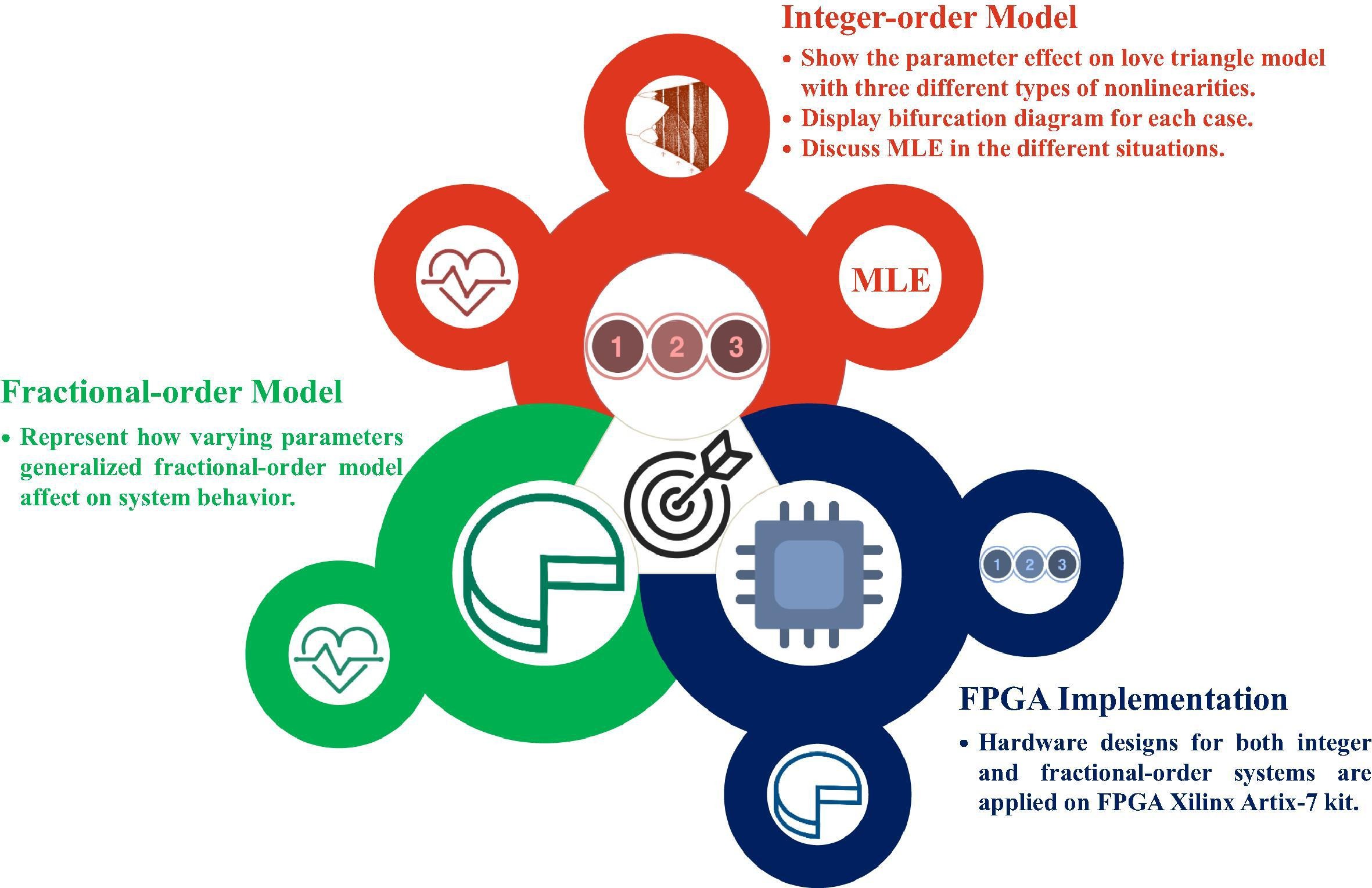
A study of the nonlinear dynamics of human behavior and its digital hardware implementation
This paper introduces an intensive discussion for the dynamical model of the love triangle in both integer and fractional-order domains. Three different types of nonlinearities soft, hard, and mixed between soft and hard, are used in this study. MATLAB numerical simulations for the different three categories are presented. Also, a discussion for how the kind of personalities affects the behavior of chaotic attractors is introduced. This paper suggests some explanations for the complex love relationships depending on the impact of memory (IoM) principle. Lyapunov exponents, Kaplan-Yorke
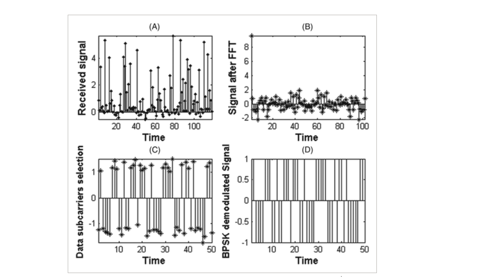
Odd clipping optical orthogonal frequency division multiplexing for VLC system
The Orthogonal Frequency Division Multiplexing (OFDM) has emerged as one of the promising techniques because of its robustness to multipath fading with high-speed data transmission. Classical bipolar OFDM cannot be used in intensity modulated with direct detection (IM/DD) optical communication systems, as visible light communication (VLC), so many optical modulation techniques as asymmetrical clipped optical OFDM (ACO-OFDM) and DC-Clipped OFDM (DCO-OFDM) have been investigated. In this paper, we introduce a novel optical modulation scheme that meets the optical communications requirements. The
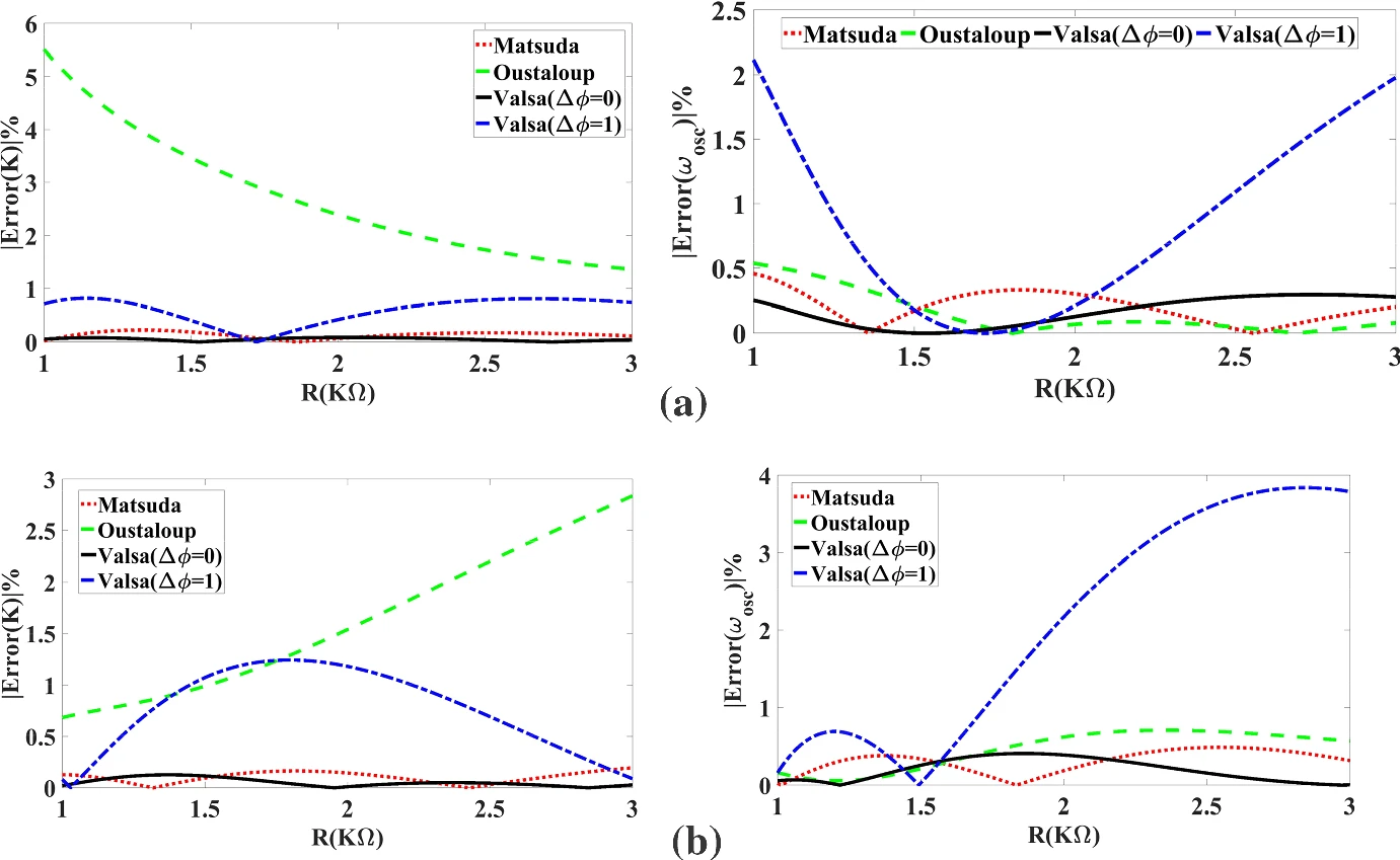
All Possible Topologies of the Fractional-Order Wien Oscillator Family Using Different Approximation Techniques
This paper introduces all the possible topologies of the Wien bridge oscillator family. This family has 72 topologies, 24 of them contain only RC or RL pairs, and the rest contain mixed pairs. The complete mathematical analysis of all twelve possible capacitive-based topologies is proposed in the fractional-order domain. The investigated circuits can be categorized into two groups, each with a similar characteristic equation. Three integer-order approximation techniques for the Laplacian operator sα are employed to solve and simulate the Wien bridge system. The studied approximations are those
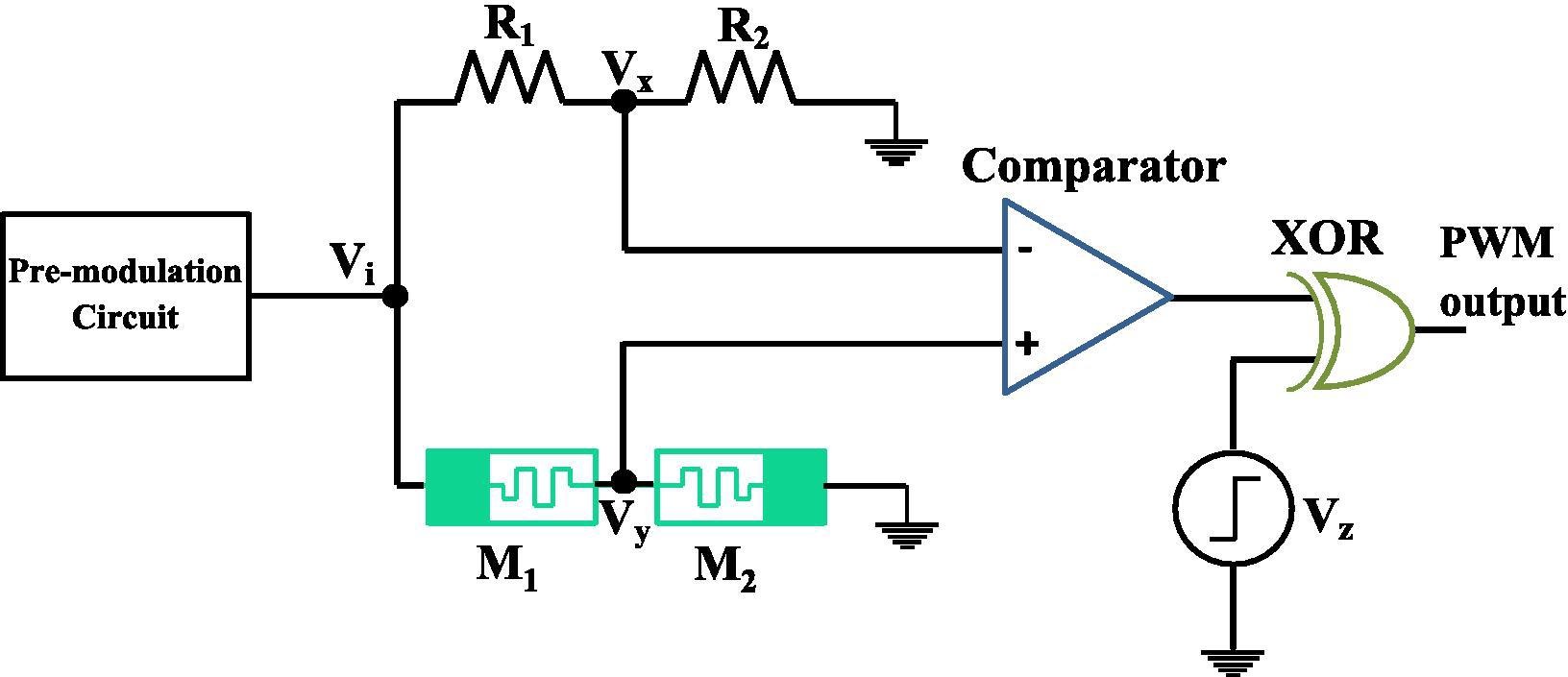
Center pulse width modulation implementation based on memristor
This paper introduces two new versions for memristor-based center pulse-width modulator (PWM) circuits. The proposed circuits use only one comparator which reduces the circuit complexity and power dissipation compared to a former work. The first design is based on two memristors and two resistors while the second design is based on four memristors. Theoretical analysis is provided, and the numerical solution is handled on MATLAB. Simulation is carried out on Cadence software, and the results follow the theoretical analysis. The experiment is implemented using commercial off-the-shelf
Pagination
- Previous page ‹‹
- Page 26
- Next page ››
